Understanding effects of Electromagnetic Interference on Structured Cabling

Tags: cabling | EMC | Noise | UTP vs STP
Today, organizations rely heavily on their computer networks, in fact few can efficiently operate without it. Once the investment and the commitment has been made, reliable operation of the network is essential. Upset of a system can not only be disastrous in terms of lost business or reduced productivity but confidence in the system quickly declines and the user either operates around the difficulty.
Modern electronic systems will in general have an unwanted response to high frequency noise signals occurring in the system by either conduction down interface cables, from another system, or induction by an electromagnetic field. In addition, systems that make use of digital electronics will contain circuits that are switching currents and voltages at high speeds and thus causing significant levels of high frequency electromagnetic radiation.
This article aims to raise the understanding of Electromagnetic Compatibility or EMC, and in particular addresses the relevance of EMC for cabling.
Electromagnetic Effects
Electromagnetic effects fall into two broad areas. The first concerns the susceptibility or immunity of electronic equipment to upset or damage by electromagnetically induced voltages and currents. The second concerns the problem of unwanted emissions of electromagnetic noise.
The present day use of electronics has expanded to such an extent that the reliability and freedom of systems from upset can now have significant implications on safety, productivity, reliability, reputation and inconvenience.
In addition to an equipment’s or system’s susceptibility to electromagnetic radiation, it is important that significant levels of electromagnetic emissions, outside the normal required signals are not produced, either as a conducted or radiated signal.
What is Electromagnetic Interference?
Electromagnetic Interference (EMI) is an all embracing term for the cause of temporary or permanent upset of electronic systems by either the naturally generated or man-made electromagnetic environment in which the system is immersed or by the unintentional induced currents and voltages being fed to equipment via interface cabling from other equipment.
EMI can also be produced inadvertently by electronic and electrical systems as a result of high frequency currents flowing within the system. If a system is designed to withstand electromagnetic threats and does not emit electromagnetic radiation above some pre-described level then the system design is said to have achieved ‘Electromagnetic Compatibility’ (EMC). The EMC of a system is the unwanted side of its performance.
It would be prohibitively expensive to protect every piece of equipment from all possible electromagnetic threats. A clear understanding of the level of protection required, and an appraisal of the electromagnetic environment in which the equipment will operate, are the first steps in the design process.
Emissions
Time varying charge distributions and current flow produce electromagnetic waves. All electrical and electronic equipment and systems involve conductors which support time varying currents and voltages and are therefore producing electromagnetic radiation to a greater or lesser degree depending on the following factors:
- The magnitude of the time varying currents flowing
- The length of the conductors
- The rate of change of the voltages and currents
- The geometrical layout of the conductors in the system in relation to each other and the earth reference.
It should be noted that even D.C. and very low frequency systems are capable of emitting significant electromagnetic radiation since rapid changes of current and voltage occur during switching operations. This can produce a transient interference source.
Susceptibility
In order to look at the reasons for the increasing susceptibility of modern electronics we must consider the huge advances in miniaturisation. These steps forward have required a massive reduction in the amount of power required to carry out a task of given complexity; this has meant that the voltages and currents used in the signalling within and between the equipment has been greatly reduced. Unfortunately, this makes the interference signals more significant by comparison. In addition to the reduction in power levels the miniaturisation has resulted in the closer proximity of one area of equipment with another, thus increasing the chance of interference.
An additional contributory factor to the increasing susceptibility of systems is the increase in bandwidth of circuitry which has arisen because of the requirement for faster processing speeds. As mentioned earlier, this produces unwanted EM emissions but also causes systems to respond in an unwanted manner to a broader range of frequencies.
In addition to magnetic components of electromagnetic fields coupling with loops contained in an electronic system to produce induced voltages, any significant length of conductor aligned with, or normal to the electric field component will have current induced in it. Systems which operate on signal levels of up to a few volts and/or currents of a few microamps, will be susceptible to electromagnetic fields unless steps are taken to prevent susceptibility. Many of the steps taken to avoid problems with susceptibility will also reduce the electromagnetic emissions.
Solutions to the EMI Problem
A full solution to the problems posed by electromagnetic interference will depend, as has been stated, on the nature of both the equipment as well as the emission specification to be met.
Each and every aspect of the design needs to be considered, starting at the board level and working outwards through the connectors to the enclosure and then on to the power supply and interface cabling.
The following are all areas of design that can enhance the overall system performance, both for active electronics and the cabling system:
- PCB Design
- Cabinet or Enclosure design
- Connector Technology
- Power Supply and Interface Cabling
It is the design of the interface cabling which is discussed in this article.
EMC and Structured Cabling
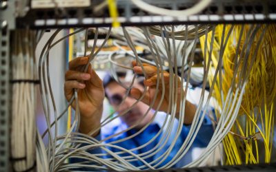
It is problematic to test an installed cabling network for EMC as most cable installers install a passive system (i.e. cable, connectors, patch panels, and outlets). Computers and communications devices are then plugged in to the installed cabling system by the owner of the network, this is not under the direct control of the cable installer. EMC must primarily be the responsibility of the manufacturer of the computer and communication equipment that is to be connected into the network. The network cabling is well defined (Category 5e and 6 for example) so manufacturers of computer equipment have a well-defined connection environment to work with.
EMC performance of the Structured Cabling may be taken into account in the following ways:-
- Manufacturers of electronic equipment/systems should take account of Generic Customer Premises Cabling in EMC Qualification. Manufacturers then qualify their product descriptions for attachment to different types of cables, for example Category 5e or 6 UTP.
- Cabling System Suppliers who also provide a “systems integration” service (and guarantee the overall performance of the system) assume responsibility.
Methods of Overcoming EMC
The particular problem for networks is due to the interconnection with extensive cabling systems. A cable, as far as Electromagnetic signals are concerned, is nothing more than an antenna that will effectively radiate any common-mode signal appearing on it, so the primary aim in network design must be to effectively limit such signals.
There are two common approaches providing EMC performance for a communications link (excluding fiber optic cabling) – screened or shielded twisted pair cabling and unshielded twisted pair cabling.
In principal it would seem that shielded systems would offer the best EMC control method by enclosing the entire link in metal. With this scheme, external noise causes currents to flow in the shield that induce equal and opposite currents in the signal conductors. These currents flow through the impedance of the conductor and shield, producing noise voltages. When summed around the loop including the ground connection of the shield, the noise voltages on the conductors cancel the voltages on the shield. Unfortunately for shielded cabling to be effective the shields need to be properly earthed at each end and this is usually in conflict with safety or other issues. Also it is difficult to ensure the continued maintenance of the screening integrity of a complex installation. Shielding utilizes the ‘Faraday cage’ approach where a conducting shield/screen is placed around the conductors and all the associated interfaces. However, this approach relies heavily on the total integrity of the conducting shield plus how and where the shield is grounded. One must remember the fact that a shield is also a conductor and if it is not treated properly as a shield, it will carry a signal, and radiate or pick up noise like any other conductor. The following conditions must be met when considering a shielded premises cabling system :
(a) Proper cable shield/screen design.
(b) Proper connector design.
(c) Proper termination of cable shield at connector.
(d) Careful installation procedures.
(e) Availability of clean power supply.
(f) Availability of good ground system.
(g) Good grounding procedures.
(h) Maintain low impedance to ground.
The effective use of unshielded cables depends on the balance of the cable itself and more importantly on the balance of the interface circuit. The differential signal is placed on a pair of wires at the transmitter, and the two wires in the pair are twisted together and closely matched over the entire link. Using this technique, any external noise will affect both wires in the pair identically (called common mode noise). At the receiver, the differential signal on the pair is interpreted as the data, while the common mode noise can be largely cancelled or filtered and ignored. This is taken into account with the design of the interface port circuit, as this is where the conversion from the wanted differential data signal to the unwanted common-mode (radiating) signal tends to occur.
The purpose of balanced transmission is to ensure that equal and opposite signals are generated on the conductors of a twisted pair. These signals, in turn, generate equal and opposite electromagnetic fields that cancel each other and the net result is no emissions from the twisted pair. Balanced transmission also makes the noise pickup equal on both conductors and so no net noise signal is delivered to the receiver interface. In general, the better the balance of the system, the lesser is its emissions and the greater is its noise immunity. The ‘balancing’ approach is often overlooked as a cost effective way of improving EMC performance. The common-mode termination techniques on the unused pairs (performed within the electronics equipment) can be considered to be a special form of balanced transmission. Its purpose is to provide the pairs with a well-defined common-mode impedance to ground, to reduce the loop (antenna) area for the common-mode signal and to balance the unused pairs. This method of termination has been shown to greatly improve the EMC performance of a system. It is currently recommended by LAN standard committees for all high data rate applications.
In reality, no system can be perfectly shielded or perfectly balanced. As with most technical issues, there is an engineering trade-off that must be evaluated to produce an optimum answer for a given set of conditions. A balanced unshielded system puts most of the emphasis of achieving acceptable immunity on the design of the interface electronics and the cabling components (cable, connector, and interconnect hardware), something that is already standard practice for electronic designers to ensure the equipment’s best EMC performance. In return for this now common design effort, an unshielded system is generally easier and less costly to install and maintain. On the other hand, a shielded system emphasises the signal path itself over the endpoints. The shielding of a link must be maintained from transmitter to receiver, including the endpoint electronics; otherwise, the effectiveness of the shield is greatly reduced. System defects must be assessed at each link by installers. Verifying the shield integrity is extremely difficult in an installation, and so defects are not readily detected or corrected. Furthermore, the design and construction of the shield plays a role in the performance, as well as cost, of the cable.
If you are interested in learning more about structured cabling, take a look at the Network Cabling Fundamentals courses available.

Written by James Donovan
You might also enjoy
FO Connector Contamination – A Constant Threat
Fiber optic communication most commonly works in duplex or multifiber transmission by transmitting light to a receiver in one direction on a fiber and receiving transmitted light back to a second receiver on the second fiber. Most engineers can understand that and...
Why Inspect and Clean Fiber Optic Connectors?
Inspecting and cleaning of fiber optic connectors during installation and when making any patching, is essential. Any contamination on a patch cord connector will be transferred through the coupler to the connector it is mated to. Even when testing fibers with a test...

Cleaning MPOs
MPO connectors should always be inspected with a scope before they are used, be that on a patch cord or a bulkhead. If they need to be cleaned, one-click cleaners are keyed to ensure the tip only fits one way onto the connectors and is able to clean both male and...